- 您现在的位置:买卖IC网 > Sheet目录1992 > DAC8426EPZ (Analog Devices Inc)IC DAC 8BIT QUAD 10VREF 20PDIP
DAC8426
–9–
REV. C
APPLICATIONS SETUP
UNIPOLAR OUTPUT OPERATION
The output voltage appearing at any output VOUT is equal to the
internal 10 V reference multiplied by the decimal value of the
latched digital input divided by 2
8 (= 256). In equation form:
VOUT(D) = D/256 × 10 V
where D = 010 to 25510
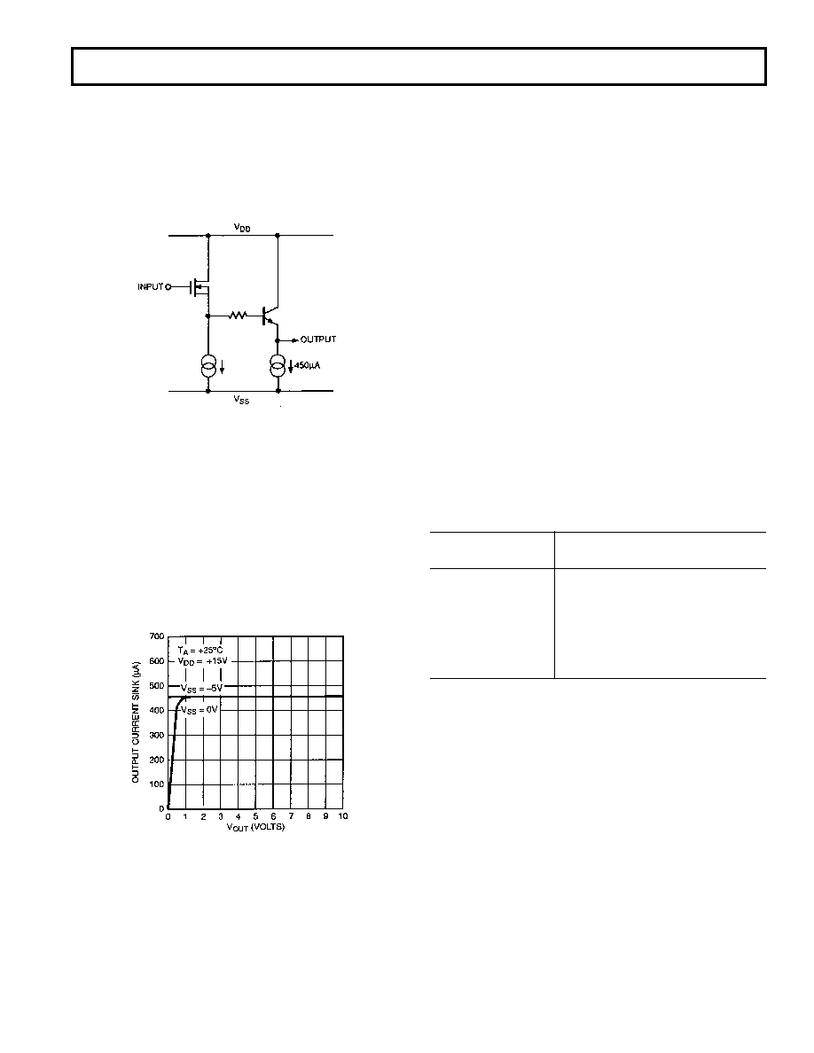
Figure 4. Amplifier Output Stage
Note that the maximum possible output is 1 LSB less than the
internal 10 V reference, that is, 255/256
× 10 V = 9.961 V.
Table II lists output voltages for a given digital input. The total
unadjusted error (TUE) specification of the product grade used
determines the output tolerances of the values listed in Table II.
For example, a
±2 LSB grade DAC8426FP loaded with decimal
12810 (half-scale) would have a guaranteed output voltage oc-
curring in the range of 5 V
±2 LSB, which is 5 V ±(2 × 10 V/256)
= 5 V
±0.078 V. Therefore V
OUT is guaranteed to occur in the
following range:
4.922 V
≤ V
OUT(128) ≤ 5.078 V
Figure 5. DAC Output Current Sink
For the top grade DAC8426EP
±1 LSB total unadjusted error
(TUE), the guaranteed range is 4.961 V
≤ V
OUT (12810)
≤ 5.039 V.
These tolerances provide the worst case analysis including tem-
perature changes.
One additional characteristic guaranteed is a DNL of
±1 LSB
on all grades. The DAC8426 is therefore guaranteed to be mon-
otonic. In the situation where a continuously positive 1 LSB
digital increment is applied, the output voltage will always in-
crease in value, never decrease. This is very important is servo
applications and other closed-loop feedback systems. Finally, in
the typical characteristic curves, long term output voltage drift
(stability) is provided.
BIPOLAR OUTPUT OPERATION
An external op amp plus two resistors can easily convert any
DAC output to bipolar output voltage swings. Figure 6 shows all
four DACs output operating in bipolar mode. This is the general
expression describing the bipolar output transfer equation:
VOUT(D) = [(1 +R2/R1) × D/256 × 10 V] –R2/R1 × 10 V,
where D = 010 to 25510
If R1 = R2, then VOUT becomes:
VOUT (D) = (D/128–1) × 10 V
Table III lists various output voltages with R1 = R2 versus digital
input code. This coding is considered offset binary. Note that
the LSB step size is now 20 V/256 = 0.078 V, twice as large as
the unipolar output case previously discussed. In order to minimize
gain and offset errors, choose R1 and R2 to match and track
within 0.1% over the selected operating temperature range
of interest.
Table II. Unipolar Output Voltage as a Function of
Digital Input Code
Digital Input
Analog Output
Code
Voltage (= D/256
× 10 V)
255
9.961 V
Full-Scale (FS)
254
9.922 V
FS-1 LSB
129
5.039 V
128
5.000 V
Half-Scale
127
4.961 V
1
0.039 V
1 LSB
0
0.000 V
Zero-Scale
OFFSETTING AGND
Since the DAC ladder and bandgap reference are terminated at
AGND, it is possible to offset AGND positive with respect to
DGND. The 10 V output span remains if a positive offset is ap-
plied to AGND. The offset voltage source connected to AGND
must be capable of sinking 14 mA. AGND cannot be taken
negative with respect to DGND; this would forward bias an in-
ternal diode. Allowance must be made at VDD to maintain 3.5 V
of headroom above VREFOUT. This connection setup is useful
in single supply applications where virtual ground needs to be
slightly positive with respect to ground. In this application con-
nect VSS to DGND to take advantage of the extra buffer output
current sinking capability when the DAC output is programmed
to all zeros code, see Figure 7.
发布紧急采购,3分钟左右您将得到回复。
相关PDF资料
DAC8531IDRBTG4
IC D/A CONV LP 16-BIT 8-SON
DAC8562FP
IC DAC 12BIT PARALLEL 5V 20-DIP
DS1004Z-5+T
IC DELAY LINE 5TAP 25NS 8-SOIC
DS1005-125+
IC DELAY LINE 5TAP 125NS 14-DIP
DS1007S-2+T&R
IC DELAY LINE 4NS 16-SOIC
DS1010S-50+T&R
IC DELAY LINE 10TAP 16-SOIC
DS1013S-25+T&R
IC DELAY LINE 25NS 16-SOIC
DS1020S-50+T
IC DELAY LINE 256TAP 16-SOIC
相关代理商/技术参数
DAC8426ER
制造商:AD 制造商全称:Analog Devices 功能描述:Quad 8-Bit Voltage Out CMOS DAC Complete with Internal 10 V Reference
DAC8426FP
功能描述:IC DAC 8BIT QUAD 10VREF 20-DIP RoHS:否 类别:集成电路 (IC) >> 数据采集 - 数模转换器 系列:- 产品培训模块:Lead (SnPb) Finish for COTS
Obsolescence Mitigation Program 标准包装:1,000 系列:- 设置时间:1µs 位数:8 数据接口:串行 转换器数目:8 电压电源:双 ± 功率耗散(最大):941mW 工作温度:0°C ~ 70°C 安装类型:表面贴装 封装/外壳:24-SOIC(0.295",7.50mm 宽) 供应商设备封装:24-SOIC W 包装:带卷 (TR) 输出数目和类型:8 电压,单极 采样率(每秒):*
DAC8426FPZ
功能描述:IC DAC 8BIT QUAD 10VREF 20DIP RoHS:是 类别:集成电路 (IC) >> 数据采集 - 数模转换器 系列:- 标准包装:1 系列:- 设置时间:4.5µs 位数:12 数据接口:串行,SPI? 转换器数目:1 电压电源:单电源 功率耗散(最大):- 工作温度:-40°C ~ 125°C 安装类型:表面贴装 封装/外壳:8-SOIC(0.154",3.90mm 宽) 供应商设备封装:8-SOICN 包装:剪切带 (CT) 输出数目和类型:1 电压,单极;1 电压,双极 采样率(每秒):* 其它名称:MCP4921T-E/SNCTMCP4921T-E/SNRCTMCP4921T-E/SNRCT-ND
DAC8426FR
制造商:Rochester Electronics LLC 功能描述:COMPLETE QUAD CMOS 8-BIT - Bulk 制造商:Analog Devices 功能描述:
DAC8426FS
功能描述:IC DAC 8BIT QUAD W/V-REF 20-SOIC RoHS:否 类别:集成电路 (IC) >> 数据采集 - 数模转换器 系列:- 产品培训模块:Lead (SnPb) Finish for COTS
Obsolescence Mitigation Program 标准包装:1,000 系列:- 设置时间:1µs 位数:8 数据接口:串行 转换器数目:8 电压电源:双 ± 功率耗散(最大):941mW 工作温度:0°C ~ 70°C 安装类型:表面贴装 封装/外壳:24-SOIC(0.295",7.50mm 宽) 供应商设备封装:24-SOIC W 包装:带卷 (TR) 输出数目和类型:8 电压,单极 采样率(每秒):*
DAC8426FSZ
功能描述:IC DAC 8BIT QUAD W/V-REF 20SOIC RoHS:是 类别:集成电路 (IC) >> 数据采集 - 数模转换器 系列:- 标准包装:1 系列:- 设置时间:4.5µs 位数:12 数据接口:串行,SPI? 转换器数目:1 电压电源:单电源 功率耗散(最大):- 工作温度:-40°C ~ 125°C 安装类型:表面贴装 封装/外壳:8-SOIC(0.154",3.90mm 宽) 供应商设备封装:8-SOICN 包装:剪切带 (CT) 输出数目和类型:1 电压,单极;1 电压,双极 采样率(每秒):* 其它名称:MCP4921T-E/SNCTMCP4921T-E/SNRCTMCP4921T-E/SNRCT-ND
DAC8426FSZ-REEL
功能描述:IC DAC 8BIT QUAD 10VREF 20SOIC RoHS:是 类别:集成电路 (IC) >> 数据采集 - 数模转换器 系列:- 标准包装:2,400 系列:- 设置时间:- 位数:18 数据接口:串行 转换器数目:3 电压电源:模拟和数字 功率耗散(最大):- 工作温度:-40°C ~ 85°C 安装类型:表面贴装 封装/外壳:36-TFBGA 供应商设备封装:36-TFBGA 包装:带卷 (TR) 输出数目和类型:* 采样率(每秒):*
DAC8501
制造商:BB 制造商全称:BB 功能描述:Low-Power, Rail-to-Rail Output, 16-Bit Serial Input DIGITAL-TO-ANALOG CONVERTER